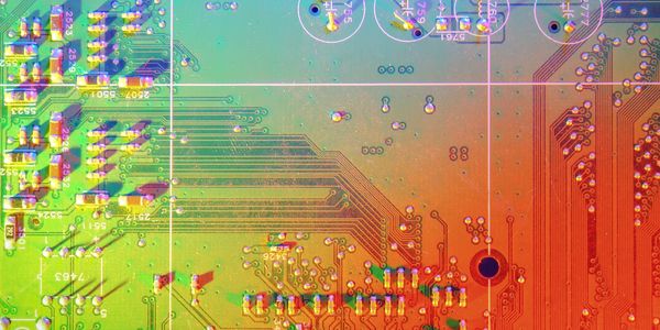
Semikons Embedded Technologies is an Embedded and VLSI Design & Development
PCB Design

Schematic Capture
Designing the logical circuit using professional EDA tools like Altium, Orcad, KiCad, DxDesigner.
Ensure accurate component selection and connectivity.
Forms the foundation for PCB layout and simulation.
Includes symbol creation and library management.
Critical for error-free downstream design processes.
Netlist verification ensures accurate PCB design by confirming that schematic connections are correctly represented in the netlist.

PCB Layout & Routing
Translating schematics into physical board design using the tools like Allegro, Altium, KiCad, Mentor Expedition.
Optimizes component placement for signal integrity and thermal management.
Includes manual and auto-routing of traces.
Supports multi-layer designs and impedance control.
Ensures manufacturability and performance.

High-Speed Design
Designing for high-frequency signals and fast data rates.
Includes controlled impedance, differential pair routing, and signal integrity analysis.
Used in applications like USB, HDMI, DDR, and RF.
Requires simulation tools and precise layout techniques.
Minimizes noise, reflections, and timing issues.
Multi-layer PCB Design
Designing boards with multiple copper layers >10.
Supports complex circuits with dense routing needs.
Improves power distribution and EMI shielding.
Used in advanced embedded systems and compact devices.
Requires careful stack-up planning, impedance and via management.

DFM & DFA Analysis
Design for Manufacturability and Assembly checks.
Ensures the PCB can be reliably fabricated and assembled.
Identifies issues like spacing violations, solderability, and component placement.
Reduces production errors and costs.
Improves yield and quality assurance.

Thermal & EMI Analysis
Simulates heat dissipation and electromagnetic interference.
Ensures components operate within safe temperature ranges.
Minimizes EMI for compliance with regulatory standards.
Uses simulation tools to optimize layout and shielding.
Essential for high-power and sensitive applications.

PCB Fabrication Support
Assistance with vendor selection and fabrication files.
Includes Gerber generation, BOM, and pick-and-place files.
Ensures compatibility with manufacturer capabilities.
Supports quality control and panelization.
Streamlines the production process.
Copyright © 2025 Semikons Embedded Technologies - All Rights Reserved.
Where business ideas take shape